New Delhi, June 18: In wake of the queries raised by the Delhi High Court about the venue of Chief Minister Arvind Kejriwal's protest at the Lt Governor's official residence, the AAP said on Monday that the party had followed proper procedures and will respond to the court.
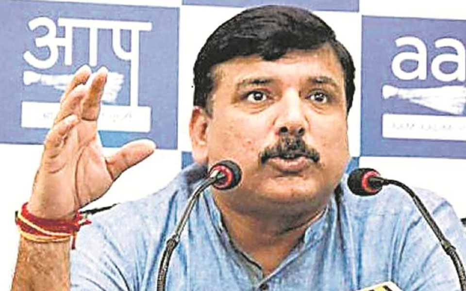
"Whatever the High Court has asked, we will answer. But I want to clarify one thing. As far as the protest at LG's office is concerned, it did not happen in just one day. We followed all the procedures, wrote letters, sent requests, did everything but ultimately, when we reached out to the LG, he did not even have five minutes to meet us," Aam Admi Party leader Sanjay Singh said in response to queries at a press conference.
The Delhi High Court on Monday sought to know from the AAP government as to who has authorised Kejriwal and his ministerial colleagues to hold a sit-in protest at the Lt. Governor's office as it was not the place to hold a demonstration.
A vacation bench of Justice A.K. Chawla and Justice Navin Chawla said: "If it is a strike or dharna, it has to be somewhere else. This can't be called a strike."
Kejriwal, his deputy Manish Sisodia and ministers Satyendar Jain and Gopal Rai had been camping in the Raj Niwas, the official accommodation-cum-office of Lt. Governor Anil Baijal, since June 11. Sisodia and Jain, who had later gone on a hunger fast, have been hospitalised following deterioration in their health condition.
Let the Truth be known. If you read VB and like VB, please be a VB Supporter and Help us deliver the Truth to one and all.
New Delhi (PTI): Congress leader Jairam Ramesh alleged on Thursday that the right to vote is under threat and the time has come when it should be made a fundamental right for citizens.
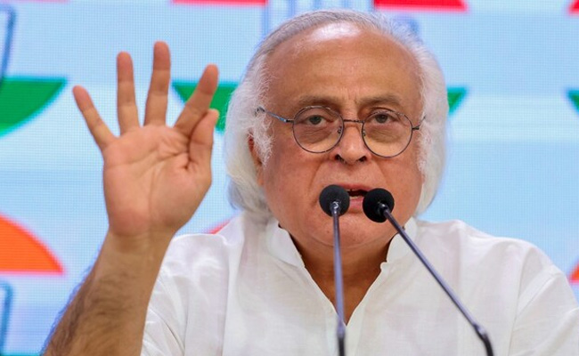
Speaking with reporters, Ramesh lashed out at Chief Election Commissioner (CEC) Gyanesh Kumar, saying the Election Commission (EC) has never been as compromised as it has been under him.
"The rot started under his predecessor. This man is a player and not a neutral observer," the Congress leader said, slamming Kumar.
Kumar is completely compromised and has become a player in elections, he alleged.
"Home Minister Amit Shah had talked about three Ds -- detect, delete and deport. So we want to know how many non-Indian citizens have been detected, how many have been deleted and how many have been deported," Ramesh said, adding that the right to vote is now under threat.
On opposition parties submitting a fresh notice in the Rajya Sabha, seeking to move a motion for the CEC's removal, the Congress leader said they will continue to make efforts for Kumar's removal as he is "compromised".
Ramesh also batted for the right to vote to be recognised as a fundamental right.
"I believe that the time has come that the right to vote should be made a fundamental right. It is a statutory right, it is not a fundamental right. Fundamental rights are justiciable," he said.
The former Union minister said this was discussed in the Constituent Assembly, but it was eventually decided that it should be made part of the Constitution.
B R Ambedkar and Jagjivan Ram had warned that in the future, governments might try to disenfranchise voters, he added.
"Once and for all, include the right to vote as a fundamental right for Indian citizens," Ramesh asserted.


